By late 2013, I had been on back-to-back overseas assignments for the Navy for 18 straight months. I missed my wife and family, and I missed the work, the people, and the environment of Arizona State University. One evening I was browsing the internet in my hotel in Bangkok, Thailand, when I happened to see a job opening at the Biodesign Institute. Upon further research, I discovered that the job requirements were an excellent fit for my knowledge and experience. I applied for the position, and my interview took place during a layover for yet another international flight. I got the position, and I eagerly joined the team at the Center for Biosignatures Discovery Automation (CBDA).
I characterize this period of my employment as the most diverse and multi-disciplinary of my entire career. My projects ranged from helping students with their thesis projects (e.g. continuous glucose monitoring), to operating and maintaining the custom Potomac laser system, to designing mechanical fixtures, electronic circuits for temperature control, sensors of virtually every type, firmware for embedded processors, microfluidic chips, devices for testing multiple cancer drugs, and too many others to enumerate.

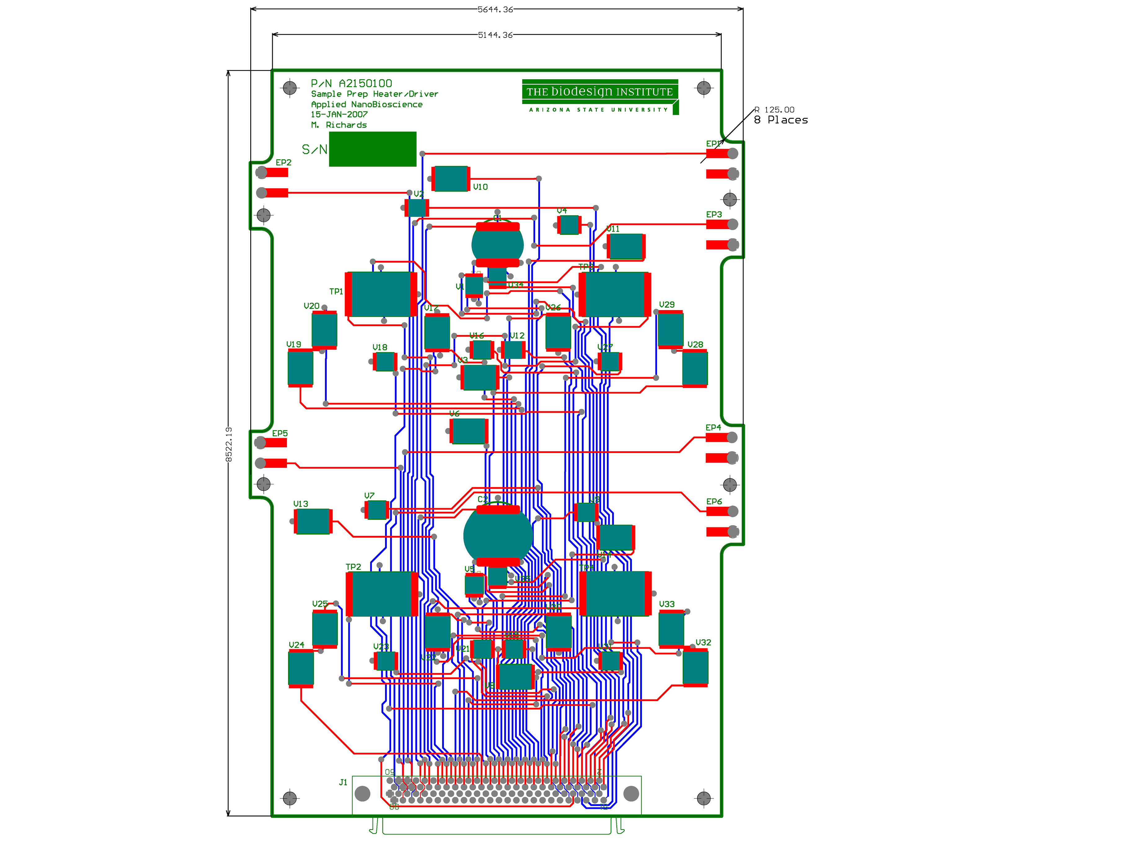
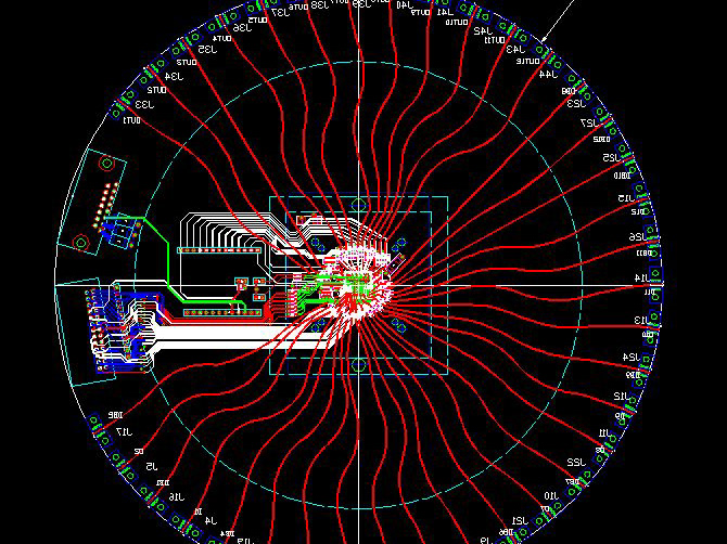
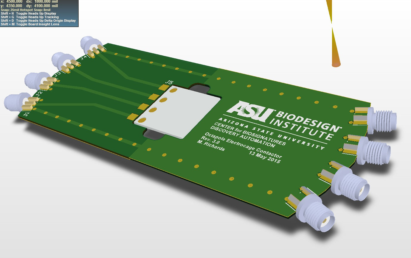
Octopole Electrocage design. 50 ohm characteristic impedance microstrip and SMA connectors.
This is my design for the "octopole electrocage" project. One of the specialties at CBDA was the 3D imaging of individual living cells. In order to image a cell in three dimensions, it has to be captured somehow, then carefully rotated. The octopole electrocage is one method of accomplishing controlled cell rotation. First, cell medium fluid is pumped through a channel in a special glass slide on custom microscope stage. Once a target cell comes into view, tiny electrodes are energized with carefully controlled pulses of electricity. The cell is rotated by changing the phase of the pulses with relation to each other. Due to the small voltages and the criticality of the phase accuracy, the design of the apparatus has to be as free from noise and cross-talk as possible. At left, you can see my design concept. I modeled the PCB in Altium Designer, and the stage and other components in Autodesk Inventor.
Here is my design, in use in the laboratory. It is immensely satisfying to see the physical manifestation of a concept. This was a case where I encountered a system that was nearly abandoned due to unreliability, lack of consistency, and non-repeatable results. I identified the root causes of the problems, then addressed them through rigrous engineering practices. The end result was extremely successful and very rewarding.
Of course, my design is just one small part of a collaborative effort. The electrocage chip was designed by a graduate student and based on previous art, and the brilliant Dean Smith designed the software to control everything.
Completed octopole electrocage system in use.
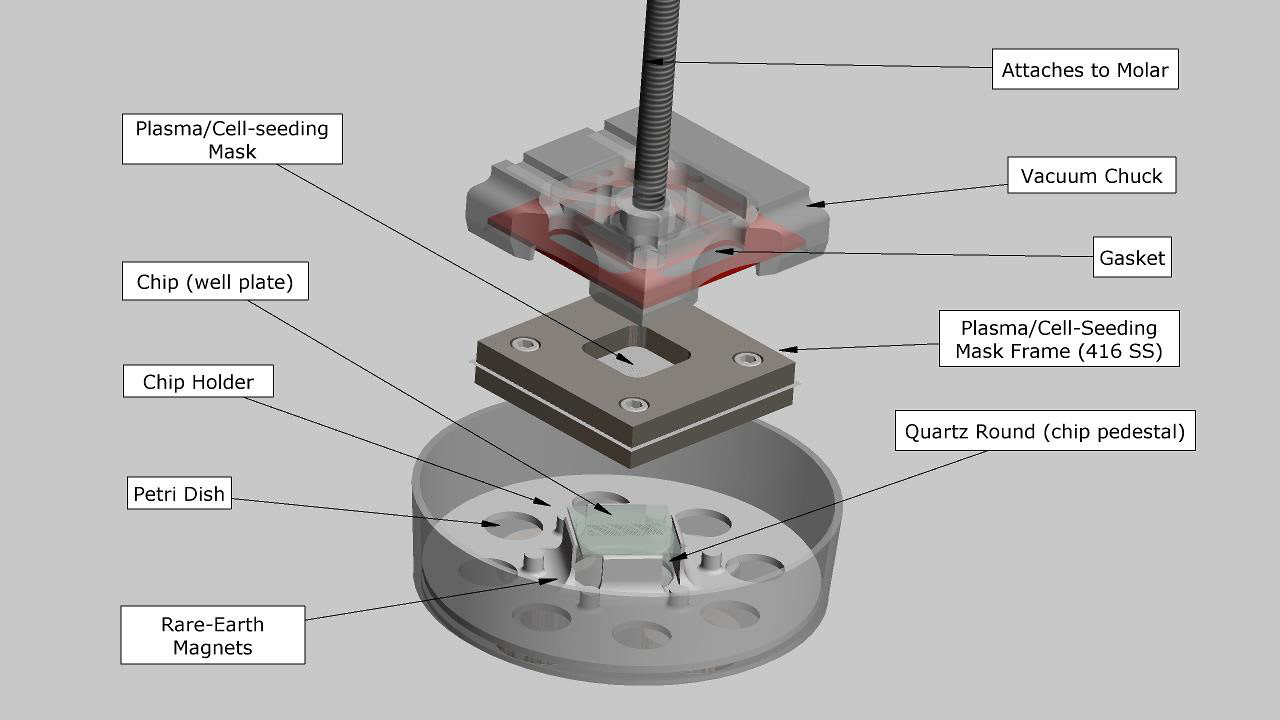
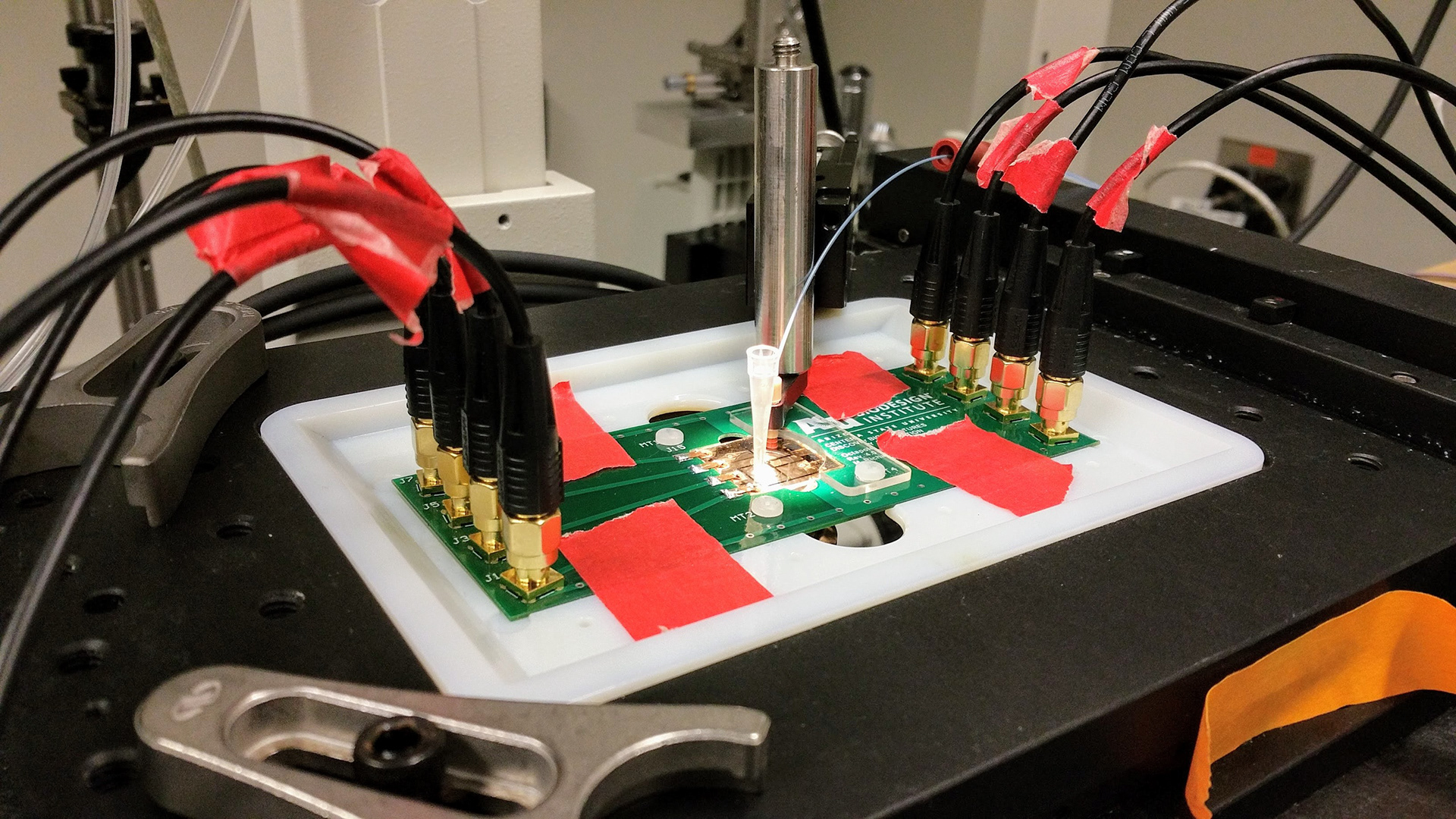
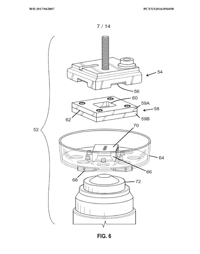
My selective cell seeding and plasma etching fixture.
This is another example of successfully engineering solutions to real-world problems. In this case, scientists needed to accomplish a few specific tasks:
1. Selectively plasma etch 1024 microscopic wells (~60um diameter) without affecting the surrounding surfaces on the glass substrate.
2. Insert living cells into those wells, quickly, without missing too many wells and without having too many wells with more than one cell each.
3. Decrease time that living cells were exposed to the air, while increasing throughput to enable more rapid testing of potential cancer treatments.
Prior to my design, the system consisted of a graduate student looking at a transparent tube through a microscope while carefully flowing cell medium through it. When a cell entered the field of view, they would move the tip of the tube to an empty well and try to deposit the cell therein.
My system worked, well enough that it was included in a patent application. The etire system consisted of a custom vacuum chuck, a magnetic stainless steel mask frame. changeable plasma/cell-seeding mask, and well plate holder assembly.
A technician looks up through the bottom of the assembly and lines up the mask with the well plate. Releasing the vacuum allows the magnets to hold the mask assembly in place. The assembly goes into the chamber for plasma etching. Once removed from the chamber, the mask frame is flooded with cell medium. the holes in the mask are carefully sized to allow optimal cell population of the wells. The well plate goes into a vision system which quickly scans the wells and automatically excludes any that are empty or contain too many cells.
The time of the entire process from plasma etch to finished cell seeding and tesing was reduced from over four hours to about fifteen minutes. This tremendously improved both throughput and the viability of the cells, since they spend far less time exposed to air.

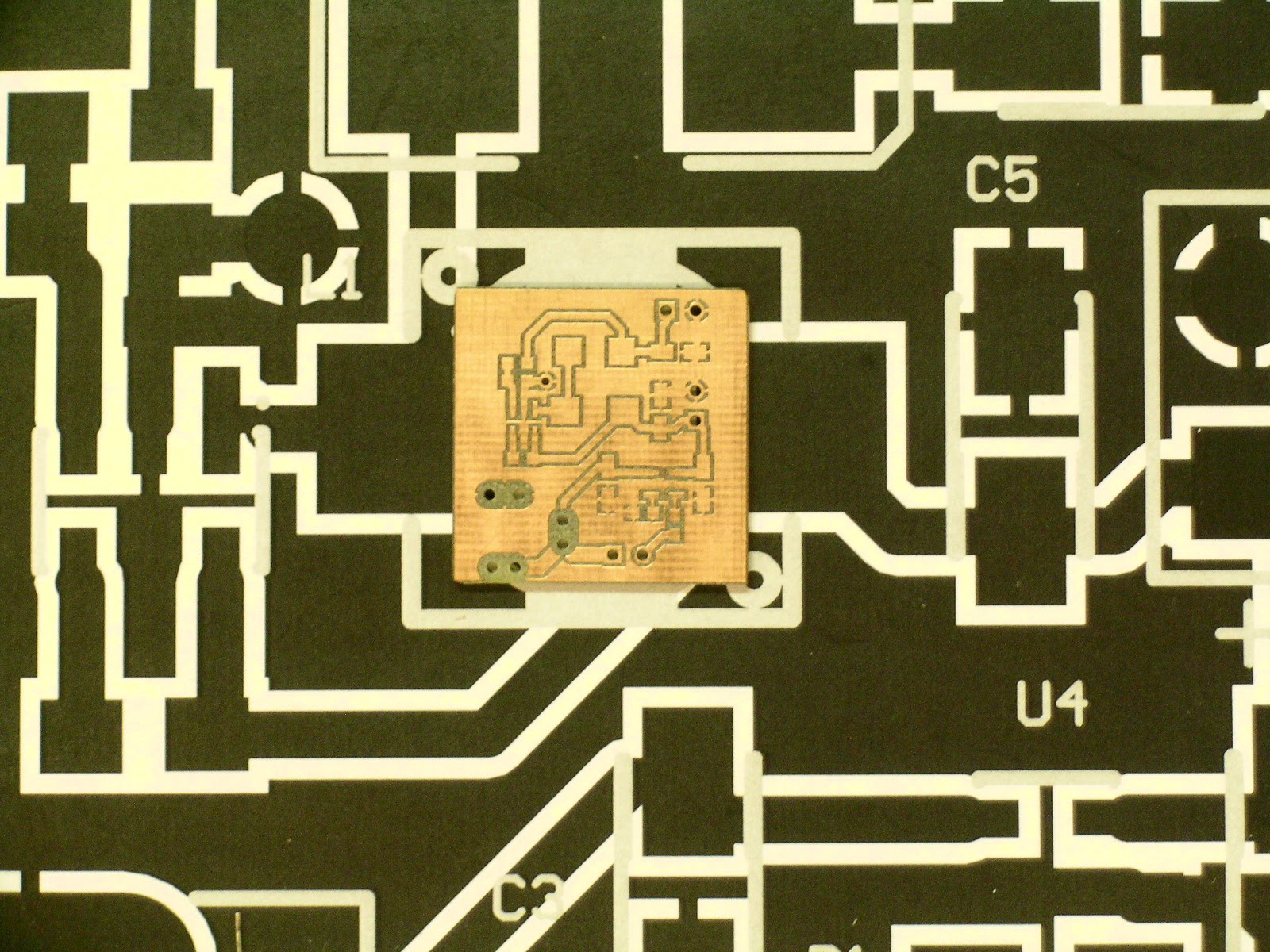
Milling a custom communications PCB
A laser-cut circuit
Early prototype of electrocage PCB

Laser-drilled holes, cell-seeding mask
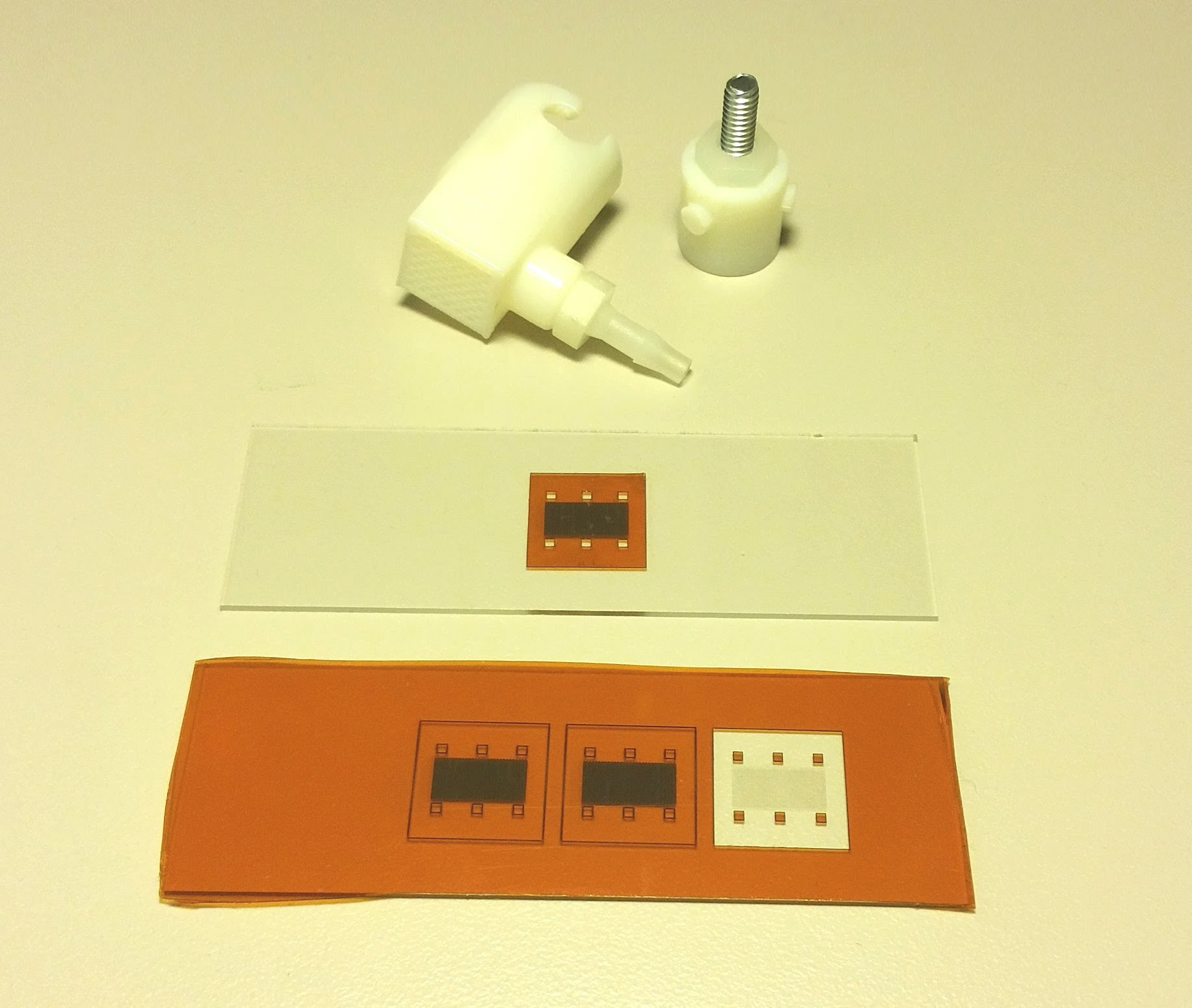
3D printed and laser cut parts
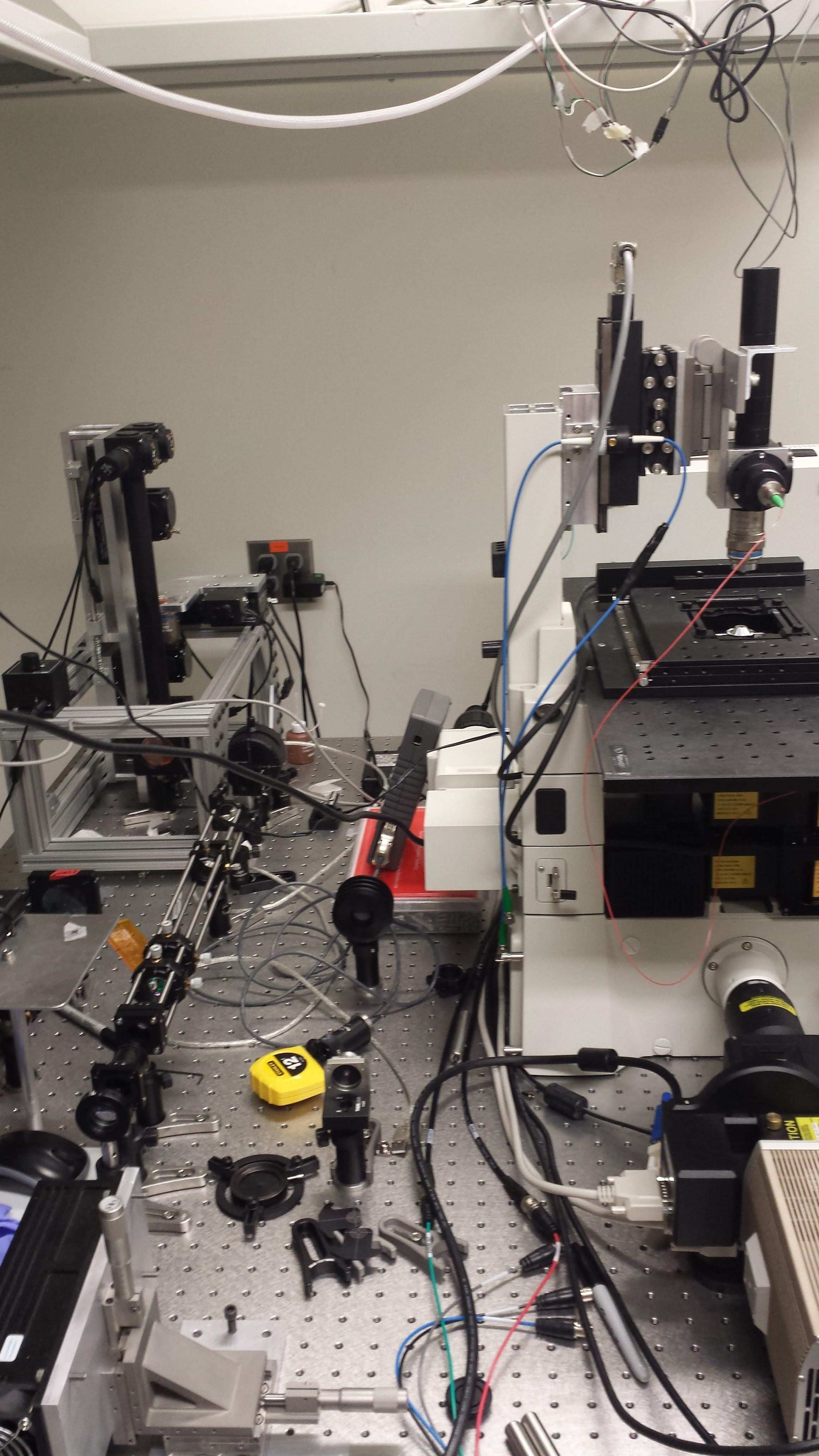
In the lab
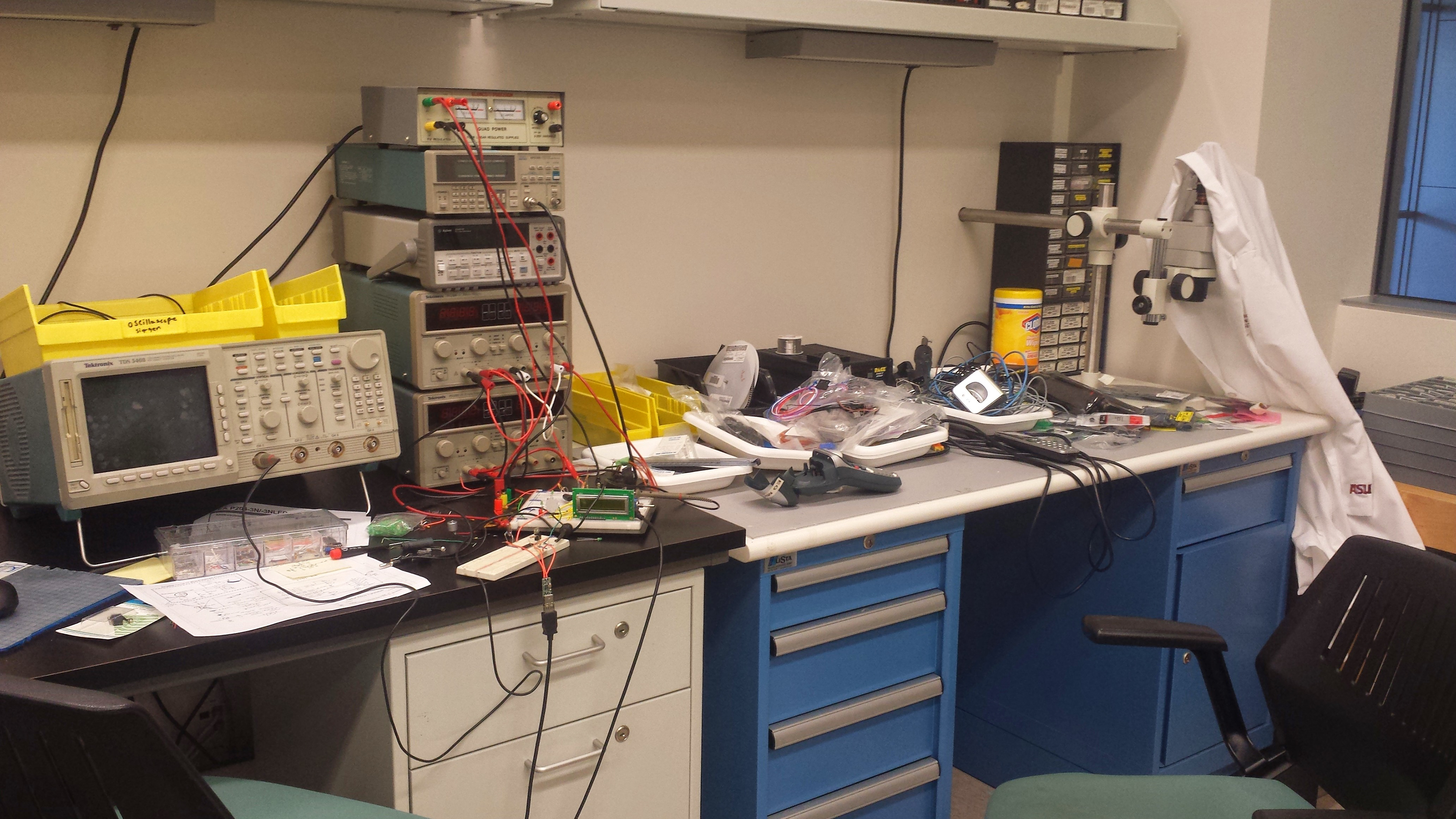
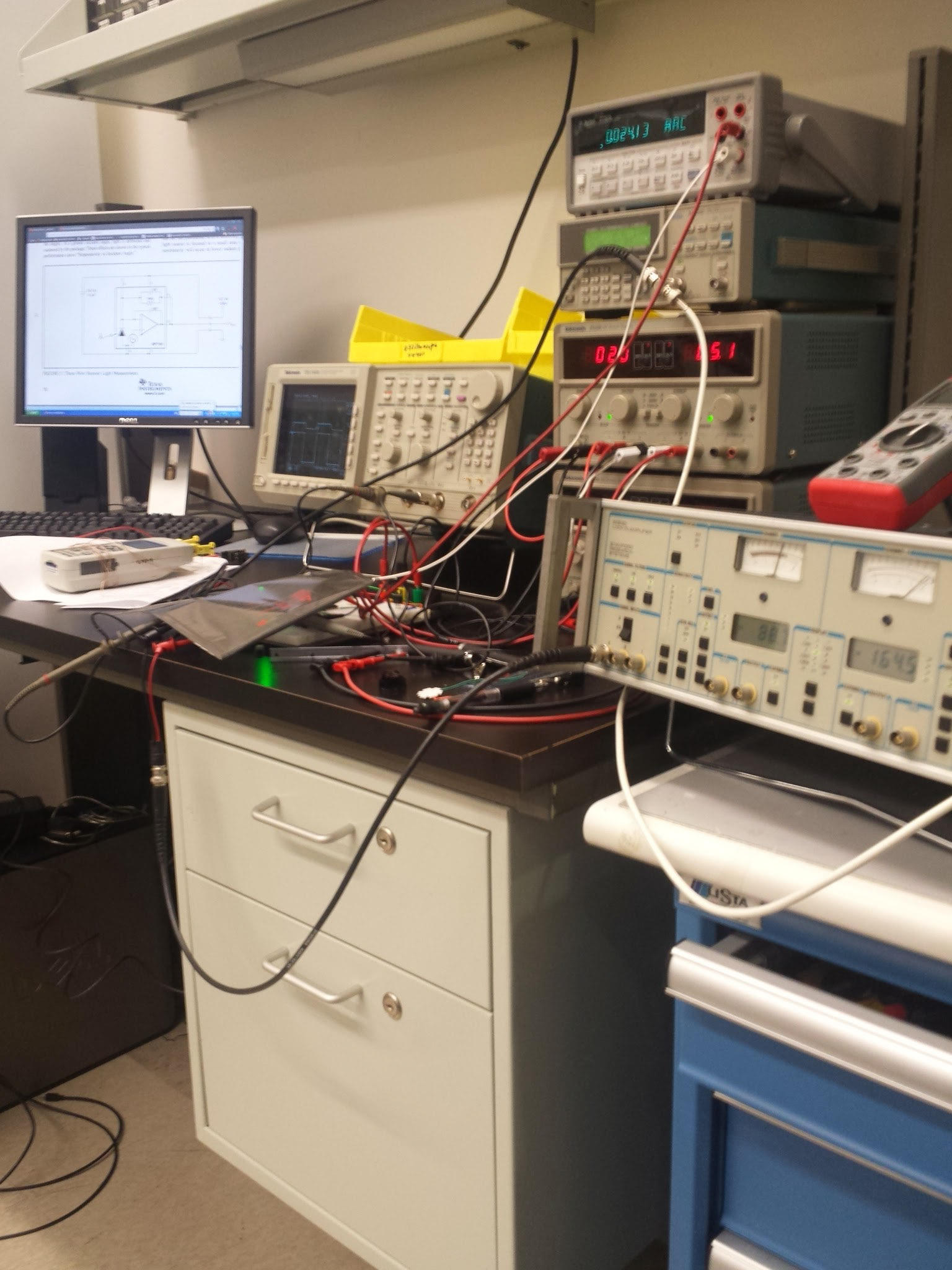
My electronics bench
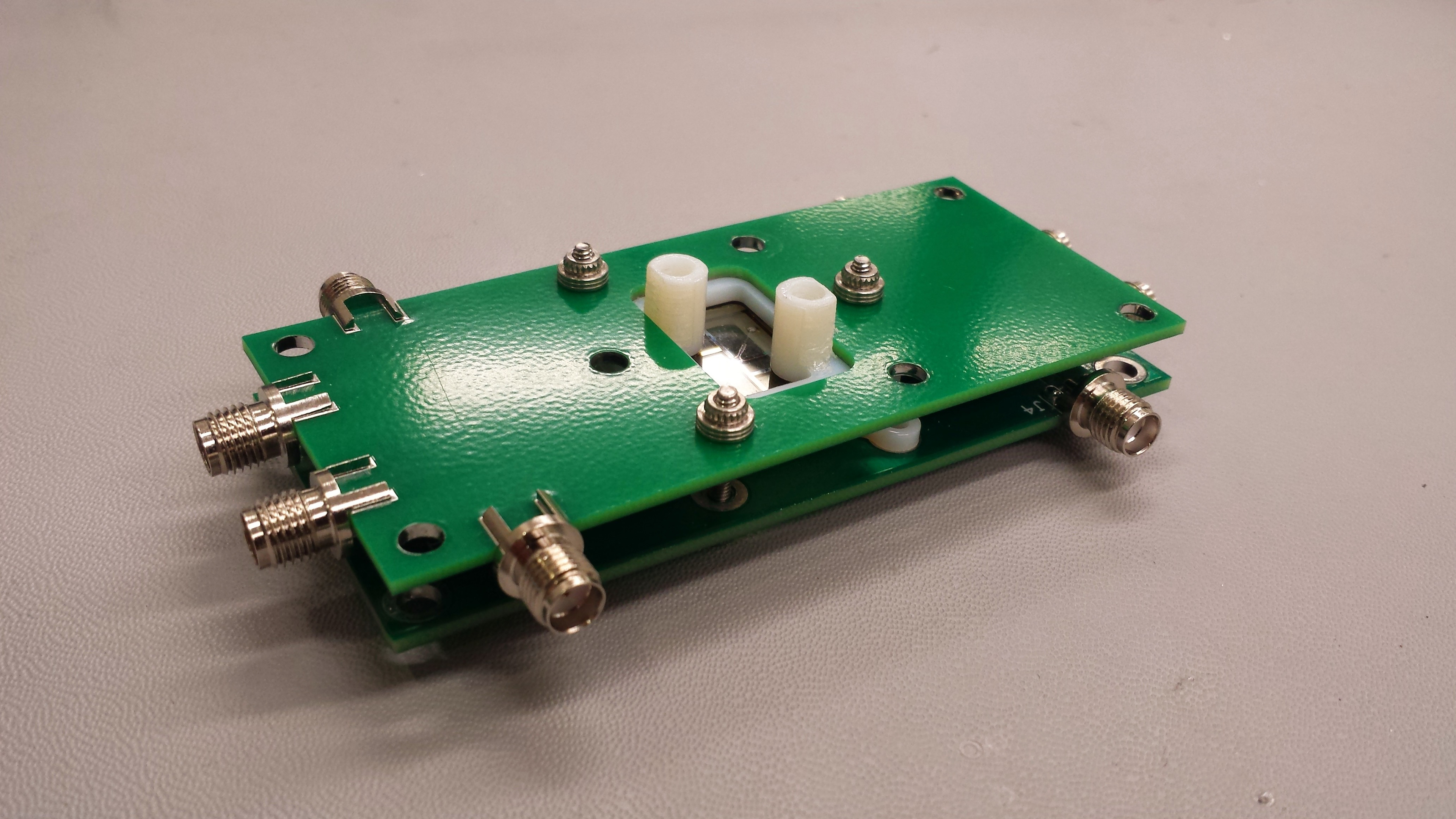
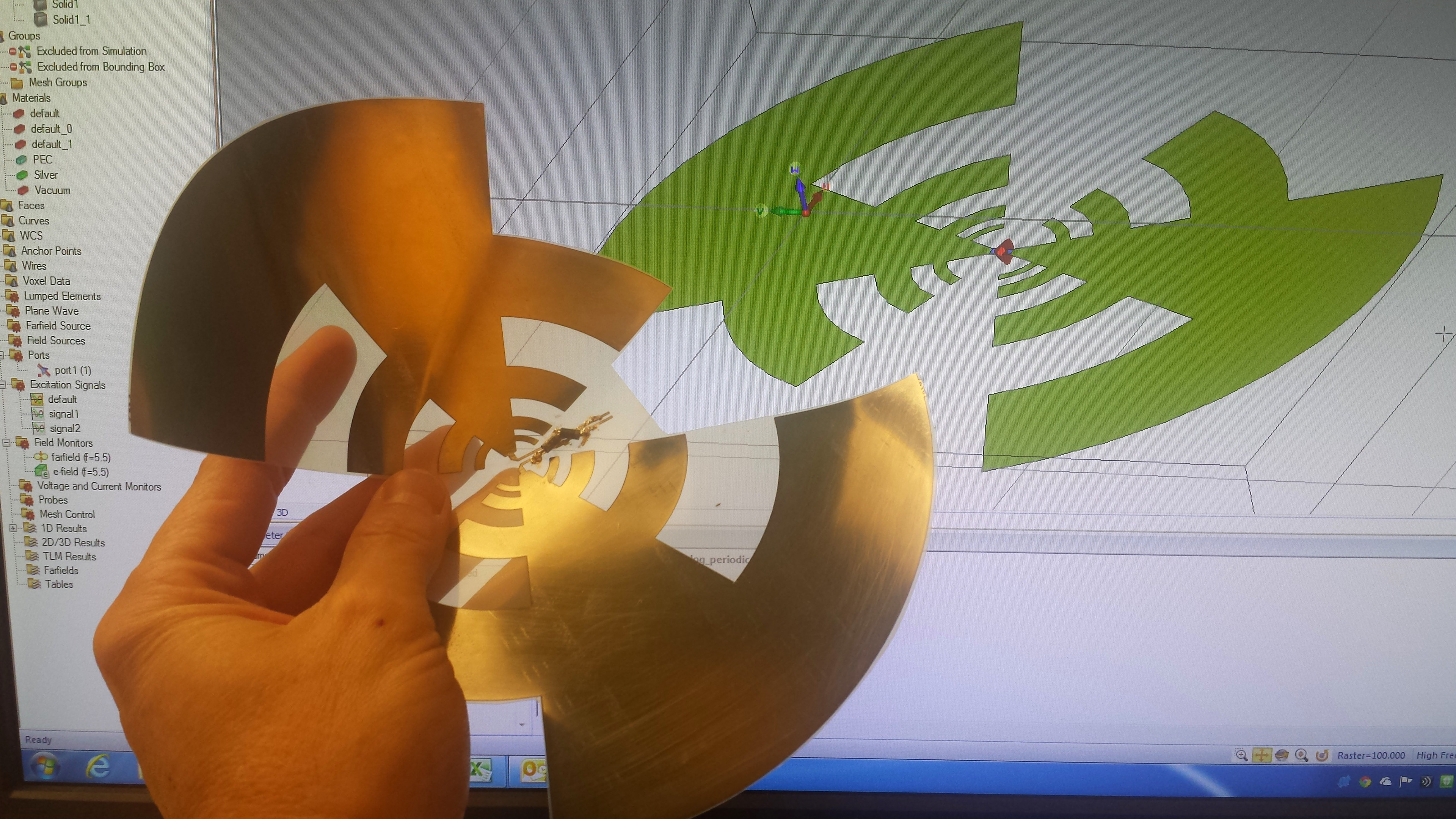
Another iteration of the electrocage design
Planar toothed antenna printed with silver nanoparticle ink.
Testing designs
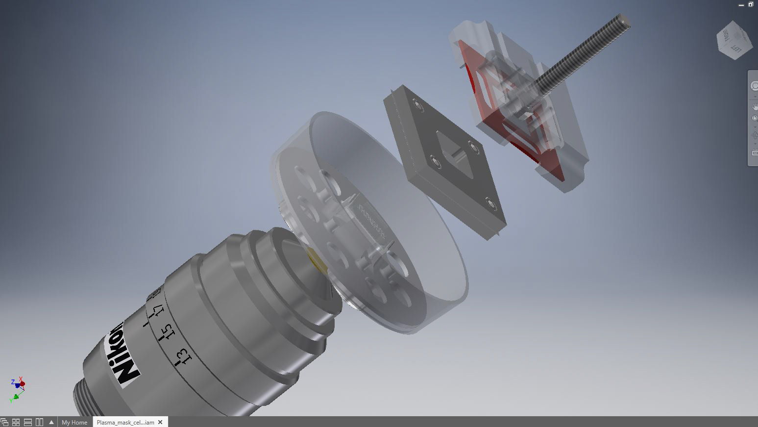
Exploded view - cell seeding assembly
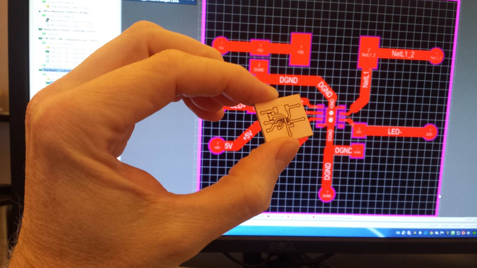
Small laser-machined circuit