I joined Motorola in 1996. I was hired by Dr. Jim Jaskie when I was fresh out of DeVry University. I left school after several semesters in their Electronics Engineering Technology program because I was starving and I couldn't find a part-time job that would work with my crazy school schedule. I had completed a few small contract electronics jobs in his laboratory, and when I left school he was kind enough to hire me full-time. I credit Dr. Jaskie for encouraging me to continue learning, and to tackle any project, no matter how far out of my depth. I continued to learn and grow as an engineer at a very rapid rate under his mentor-ship.
Over the next few years, I studied digital and analog circuit design, printed circuit design, and completed a course of study in the physical design of integrated circuits. I learned to work with ultra-high vacuum, high-voltage, video encoding, 3D modeling, and even computer networking. This was the golden age at Motorola, where creativity was rewarded and possibilities were boundless.
Although I didn't complete my formal degree plan, I eventually boarded as an engineer. The formal boarding process consisted of passing the Motorola engineering written exam, and successfully answering questions by a panel of electrical engineers and physicists.
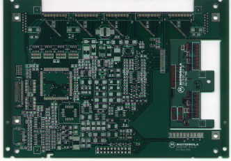
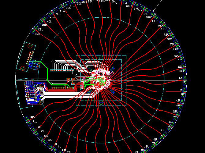
Display driver board, featuring 0.006" minimum features.
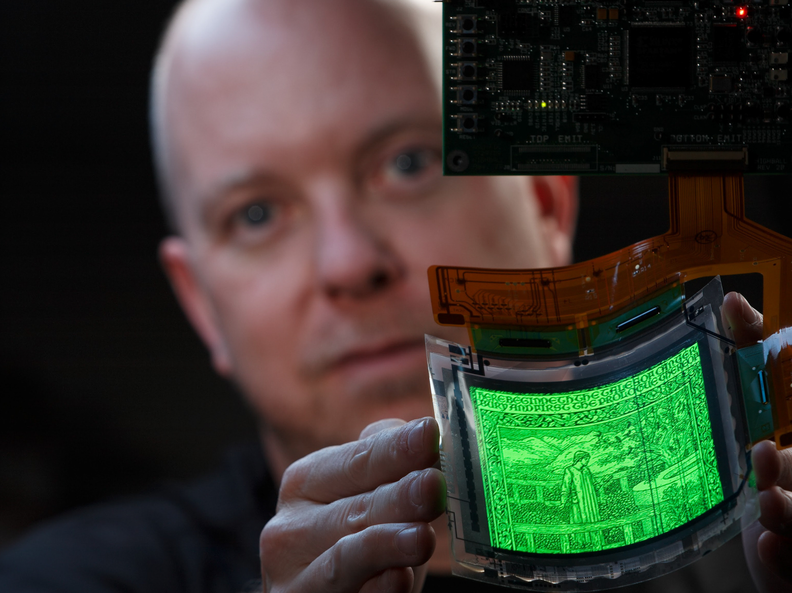
This is a 4-layer printed circuit board I designed for driving a 7" diagonal flat panel display. In the late 1990's, while working in the Motorola research laboratory in Tempe, Arizona, we demonstrated a new type of display based on Spindt Tip technology. The Field Emission Display (FED) was like a very thin CRT, with several microscopic electron guns directly behind each pixel. These emissive displays were only about 5mm thick, but they were daylight-visible and virtually unaffected by temperature extremes.
This circuit board contained logic for converting analog video into digital, column driver chips, high-voltage row drivers, level shifting circuits, and feedback to maintain constant display brightness. The boards also contain fiducials and rails for automated assembly. Material is .031" FR4.
Motorola bet $50 million on a new factory to produce these marvelous displays, but by the time we overcame all the technical hurdles to mass-produce FED's, the price of competing liquid crystal panels had plummeted. The Motorola technology never went into full-scale production.
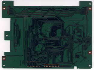
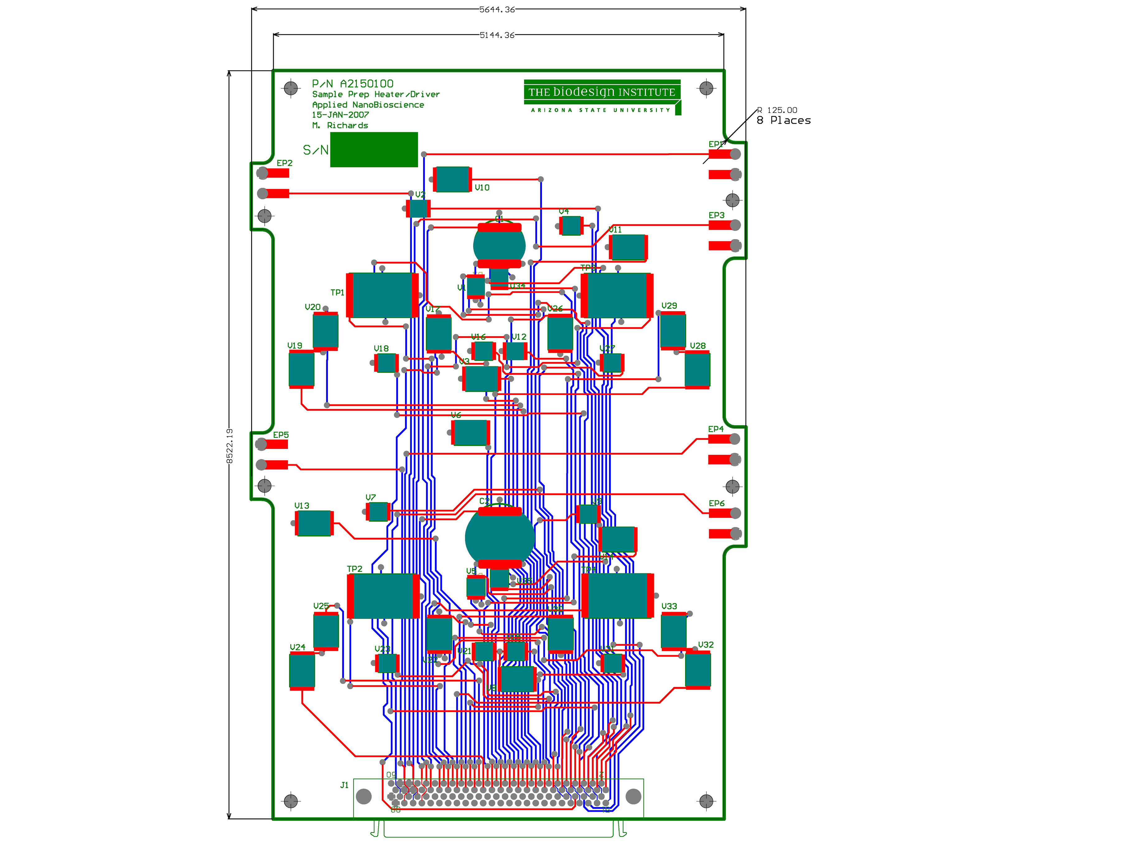
Back of display driver board. The display panel mounted to this side.
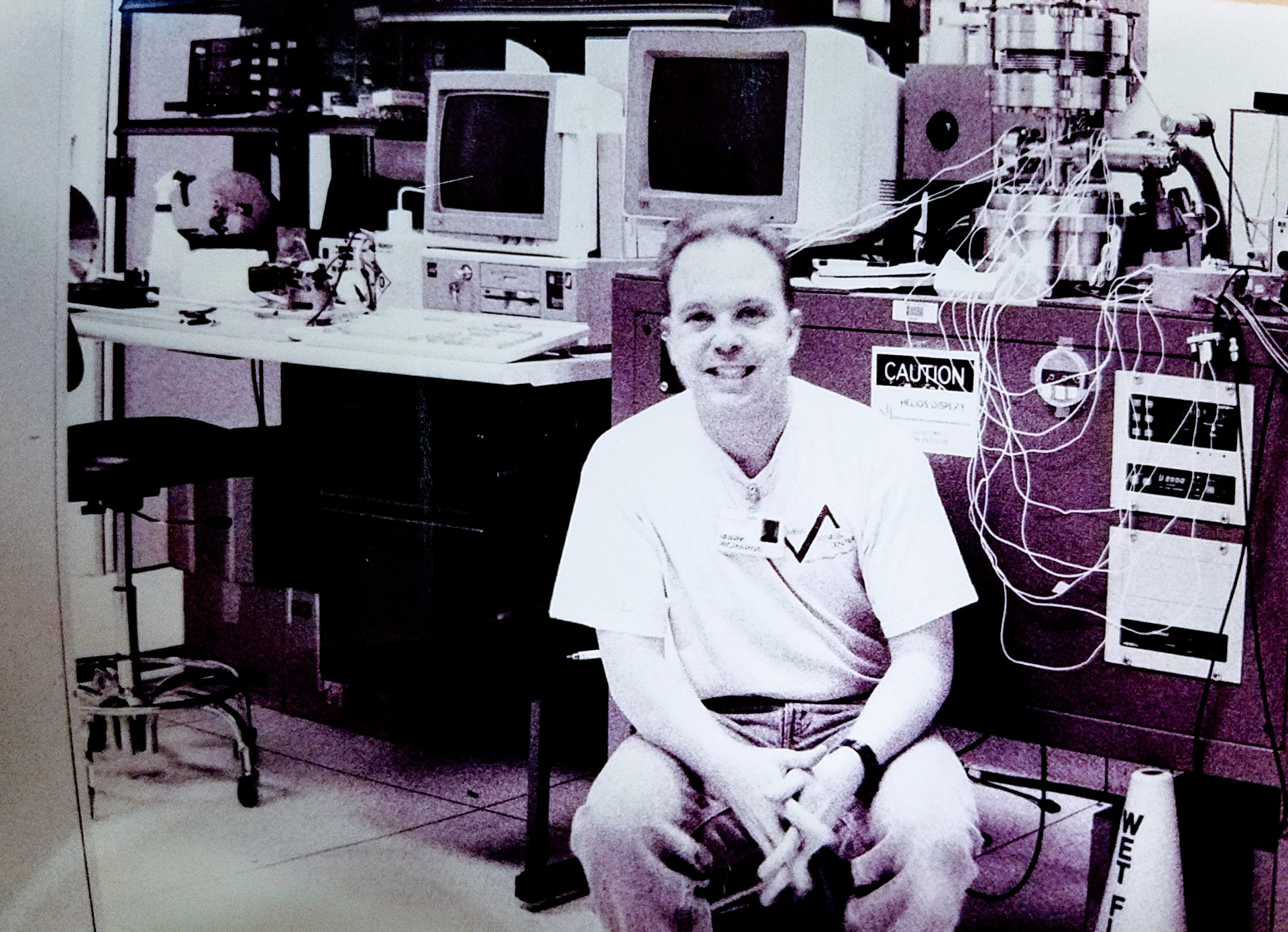
Mark at Motorola Corporate Research Lab, ca. 1996